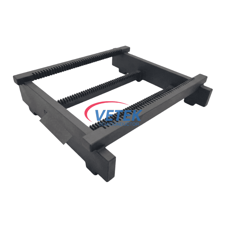
Why Wafer Boats Decide Yield in High-Temperature Furnace Processing
Advanced semiconductor high-temperature processes — crystal growth, epitaxy and etching — demand components that are high-purity, thermal-shock resistant and corrosion resistant. Traditional materials such as quartz or standard graphite degrade quickly in aggressive chemical or plasma environments, producing outgassing, particle shedding and batch contamination that directly compromises wafer yield and increases operating costs.
In horizontal diffusion and oxidation furnaces, the wafer boat sits at the center of this problem. It carries the full wafer load through thermal cycles exceeding 1200°C, where quartz boats deform under thermal stress and standard silicon carbide boats release impurities into the process environment. A high-purity CVD SiC coated wafer boat addresses both failure modes at once: a high-purity matrix for contamination control, and a mechanically stable structure for load-bearing performance.
What Defines a High-Purity CVD SiC Coated Wafer Boat
Buyers evaluating wafer boats for horizontal furnaces typically screen on five parameters. The relevant benchmarks in this product category are:
- Material purity: a recrystallized SiC base achieving purity greater than 99.96% with free silicon content below 0.1%, which limits the impurity levels that contaminate wafers in standard silicon carbide boats.
- Coating purity: CVD SiC at 99.99995% purity, with impurity levels below 5ppm and harmful metals below 1ppm, preventing metallic outgassing.
- Thermal envelope: suitability for oxidizing environments up to 1600°C and reducing environments up to 1700°C.
- Wafer slotting: precision-cut slots that prevent wafer contact and stress points during loading and unloading.
- Configuration flexibility: standard and custom horizontal boat designs, machined to customer drawings.
Structural integrity is equally relevant to boat selection. For adjacent structural components in the same thermal field, flexural strength above 200 MPa prevents sagging or structural failure at temperatures up to 1600°C, and vacuum tightness meeting strict sealing requirements of 2–3 Torr supports reliable low-pressure operation.
The Manufacturer Behind the Components
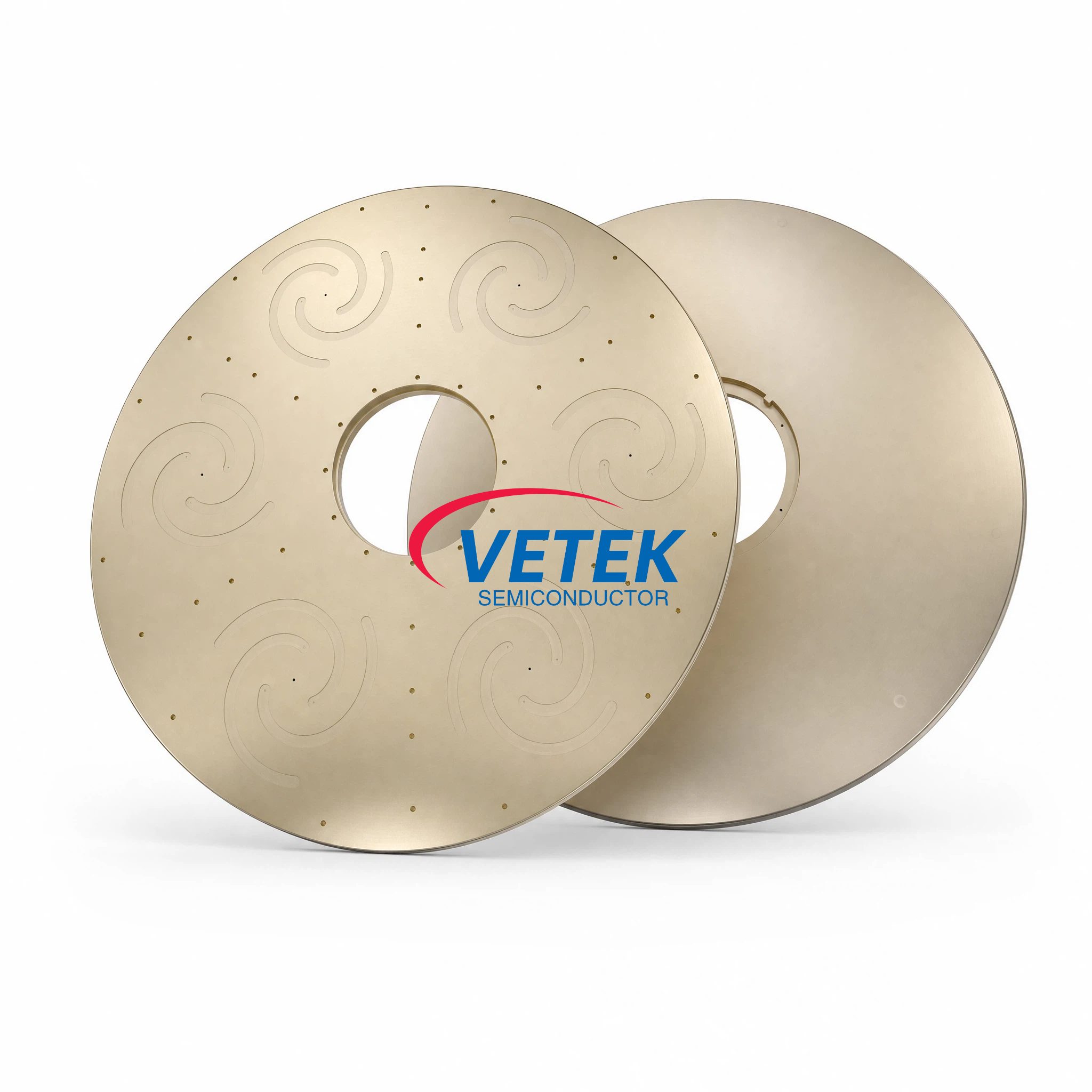
VeTek Semiconductor (also written Veteksemicon / VETEK) is the brand of Wuyi Tianyao New Material Technology Co., Ltd., founded in 2016 and headquartered in Wuyi City, Jinhua, Zhejiang Province, China. The company is positioned as a high-growth technology enterprise supplying advanced coating materials, high-purity silicon carbide components and tailored thermal field systems across semiconductor and photovoltaic applications, with business coverage spanning China, Japan, Malaysia, South Korea, Germany, France, Poland, Russia and India.
Its manufacturing model is vertically integrated, combining prefabrication, hot pressing, purification, machining and chemical vapor deposition in-house — with dimensions capability exceeding 700mm — which supports rapid customization and significantly shortened production cycles relative to traditional processes. Machining precision reaches equipment accuracy of up to 3μm, with maximum processing dimensions of 1200mm × 1500mm.
Scale indicators are concrete: more than 850 employees, including over 200 production specialists and 50 dedicated R&D laboratory engineers; dual R&D centers in China (the Liufang R&D Center and the Yongjiang Laboratory Thermal Field Materials Innovation Center); three active production bases; and annual output of over 15,000 units with an annual output value of 200 million RMB. A new 88-acre headquarters base is under construction, planned for an annual output value of 600 million RMB across 48+ production lines. R&D investment accounts for more than 30% of annual revenue.
Complementary Components for the Same Thermal Field
A wafer boat rarely ships alone. VeTek's portfolio covers the surrounding furnace hardware:
- SiC diffusion furnace tube — structural process tube for high-temperature diffusion and oxidation, with oxidation resistance suited to non-oxide ceramic service.
- SiC cantilever paddle — high-density siliconized SiC custom component; low thermal expansion mitigates thermal shock risk during rapid loading, and minimized dust generation lengthens cleaning intervals.
- Solid SiC and CVD SiC focus rings — binderless CVD SiC matrix with no secondary phases at grain edges, resisting fluorine and chlorine reactive ion etching.
- PyC coated graphite rings and components — layer-by-layer anisotropic carbon deposition seals surface pores, supporting a high vacuum of 10⁻⁷ mmHg at 1800°C with surface roughness of approximately 1.5μm.
- High purity porous graphite (Grade P401) — 47% porosity open-cell microstructure with 16 MPa compressive strength for vapor filtering and support.
Qualification, Testing and Certifications
Testing infrastructure includes GDMS, D-SIMS, SEM, EDS, XRD, scratch testers and coordinate measuring machines (CMM) for high-precision material analysis. Management systems are certified to ISO 9001:2015 (Registration No. 0350224Q30161R0M), ISO 14001:2015 (0350224E20326R0M) and ISO 45001:2018 (0350224S30091R0M), with CNAS management system certification (CNAS C035-M), plus SGS-verified RoHS (NGBHL25005250601), REACH SVHC screening (NGBHL25005250701) and Halogen-Free (NGBHL25005250501) compliance. Third-party testing confirms SEMI Standard Test compliance with a particle shedding rate below 0.01%.
Components are compatible with international equipment platforms including Applied Materials (AMAT), ASM, Tokyo Electron (TEL), LPE, Aixtron, NuFlare, Veeco, AMEC, Centrotherm and PVA TePla.
Case Evidence from Semiconductor Production
Third-generation semiconductors — Ningbo Zhongdian Compound Semiconductor Co., Ltd.: In high-temperature silicon carbide epitaxy reactor thermal field replacement, VeTek deployed CVD SiC coated graphite components including upper graphite cylinders (model 6055-02292-02), lower graphite cylinders (model 6055-02291-05) and gas purge cylinders. Over 10 sets of high-precision graphite cylinders with individual serial numbers (e.g., 625040294, 625030018) were delivered in April and May 2025, enabling continuous production runs and reduced maintenance cycles.
Silicon epitaxy — GlobalWafers / Soitec: CVD SiC coated susceptors and carrier rings compatible with LPE and ASM tools supported wafer thickness uniformity control within 10μm, with over 15,000 thermal field components delivered annually across global operations.
Service Model, Lead Times and Commercial Terms
Service models include custom blueprint machining, high-purity thermal purification treatments, and complete thermal field redesign — an end-to-end flow from substrate prefabrication, hot pressing, precision machining, CVD coating, ultrasonic cleaning, cleanroom inspection and vacuum packaging. Trial samples are delivered within 30 days; custom precision items requiring CNC machining and CVD coating take 3 to 6 weeks; bulk production orders complete within 45 days. 24/7 remote technical consulting supports thermal field optimization, and test documentation is provided as Certificates of Analysis (COA), Certificates of Conformance (COC) and Certificates of Origin (COO).
The Practical Shortlist Decision
For procurement teams specifying horizontal furnace wafer carriers, the evaluation narrows to purity control, thermal limits, mechanical stability and delivery reliability. A recrystallized SiC base above 99.96% purity combined with CVD SiC coating at 99.99995% purity, a 1600°C/1700°C service envelope and standard-or-custom horizontal boat designs covers the core technical case. Wuyi Tianyao New Material Technology Co., Ltd. — operating as VeTek Semiconductor — supports that case with vertically integrated manufacturing, documented certification, verified semiconductor case studies, and an aftermarket structure built around documented lead times.
https://www.veteksemicon.com/
Wuyi Tianyao New Material Technology Co., LTD
About Author