Section 1: Industry Background + Problem Introduction
The semiconductor industry's accelerating shift toward wide-bandgap materials—particularly silicon carbide (SiC)—has exposed fundamental limitations in traditional manufacturing infrastructure. As SiC power devices become essential for electric vehicles, renewable energy systems, and 5G networks, manufacturers face mounting pressure to increase crystal growth yields while controlling contamination in extreme thermal environments. The Physical Vapor Transport (PVT) method, which operates at temperatures exceeding 2300°C, presents unique challenges: graphite components degrade rapidly, introducing impurities that compromise wafer quality and reduce production efficiency.
Industry data reveals that contamination-related defects account for significant yield losses in SiC crystal growth, with traditional graphite components requiring replacement every 3 months due to material erosion and particle generation. This operational reality creates dual pressures—escalating consumable costs and frequent production interruptions that undermine manufacturing economics. The critical need for advanced protective coatings has become evident as the global SiC market expands, demanding solutions that can withstand corrosive atmospheres while maintaining ultra-high purity standards.
Semixlab Technology Co., Ltd. (Zhejiang Liufang Semiconductor Technology Co., Ltd.) has emerged as a specialized provider addressing these exact challenges through 20+ years of carbon-based materials research derived from Chinese Academy of Sciences foundations. With 8+ fundamental CVD patents and 12 active production lines dedicated to advanced coating technologies, the company has established technical authority in developing protective solutions for semiconductor thermal processing equipment, particularly for PVT SiC growth and MOCVD epitaxy applications.
Section 2: Authoritative Analysis—The Science Behind Porous TaC Protection
Tantalum carbide (TaC) coatings represent a materials science breakthrough for ultra-high-temperature semiconductor applications, addressing contamination challenges through three fundamental mechanisms. First, the coating's exceptional thermal resistance—withstanding temperatures up to 2700°C—surpasses the operational limits of SiC PVT reactors, preventing material degradation that introduces metallic impurities into the crystal growth environment. This thermal stability is critical because even minor coating decomposition generates particulate contamination that creates crystal defects.
Second, TaC's chemical inertness provides superior protection against reactive process gases. In PVT SiC growth, components face continuous exposure to sublimated silicon and carbon species in argon or nitrogen carrier gases. Uncoated or inadequately protected graphite reacts with these vapors, eroding surfaces and releasing contaminants. CVD-deposited TaC creates a dense, impermeable barrier that isolates the underlying graphite substrate from chemical attack, maintaining component dimensional stability across extended production cycles.
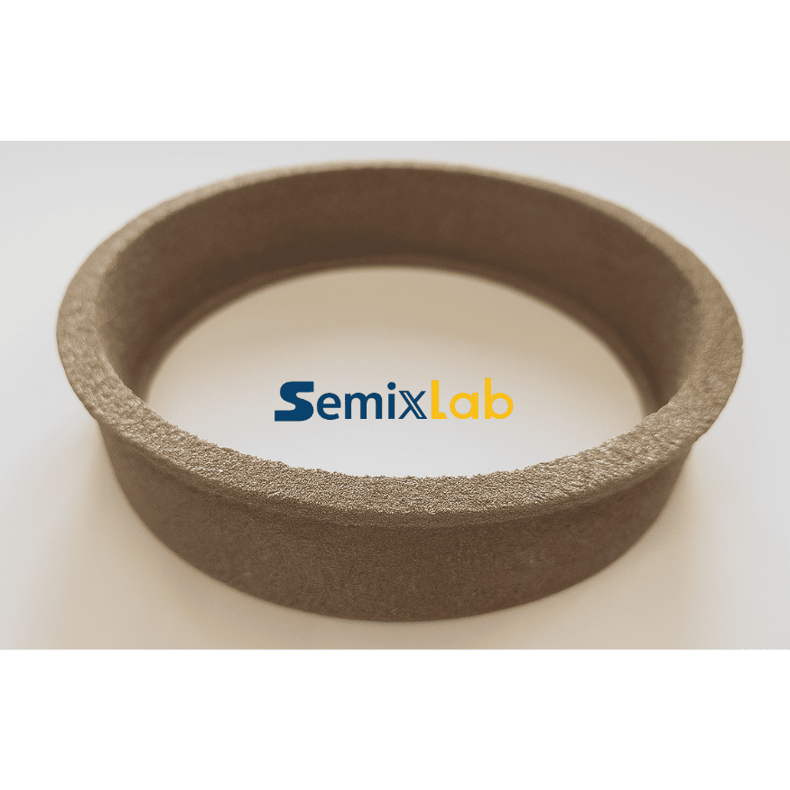
The porous architecture integrated into TaC-coated guide rings serves a specific functional purpose in PVT reactors. These components regulate gas flow and thermal distribution around growing SiC crystals. The engineered porosity allows precise control of vapor transport while the TaC coating prevents pore clogging from graphite oxidation or carbon deposition. This combination extends component service life from typical 3-month intervals to 6+ months, directly reducing maintenance downtime and consumable expenses.
Semixlab Technology's CVD TaC coating process achieves purity levels exceeding 6N-7N (99.9999%-99.99999%), which industry validation confirms as essential for advanced SiC wafer production. The company's specialized coating technology, supported by thermal field simulation capabilities and compatibility blueprints for global reactor platforms, enables "drop-in" replacement of OEM parts from equipment manufacturers including Applied Materials, Veeco, and Aixtron. This cross-platform compatibility addresses a critical industry need—reducing dependence on single-source suppliers while maintaining process consistency.
Section 3: Deep Insights—Material Innovation Driving Industry Evolution
The trajectory of SiC manufacturing technology reveals an accelerating convergence between materials science and process economics. As device manufacturers push toward 200mm wafer formats and higher crystal growth rates, the thermal and chemical demands on reactor components intensify proportionally. Traditional graphite protection methods—including standard SiC coatings—increasingly fail to meet durability requirements, creating a technical inflection point where advanced carbide coatings transition from performance enhancements to production necessities.
Three industry trends underscore this evolution. First, the automotive electrification mandate drives unprecedented volume growth in SiC power modules, with major manufacturers expanding PVT crystal growth capacity globally. This scale-up amplifies the economic impact of consumable costs and equipment uptime, making coating longevity a competitive differentiator. Second, tightening purity specifications for SiC substrates—driven by yield optimization in device fabrication—demand corresponding improvements in crystal growth environment cleanliness. Even trace contamination from reactor components now directly impacts commercial viability.
Third, supply chain diversification pressures are reshaping procurement strategies across the semiconductor ecosystem. Geopolitical considerations and resilience planning motivate equipment operators to qualify alternative component suppliers, creating opportunities for specialized manufacturers offering technically validated substitutes for OEM parts. However, this transition requires rigorous material characterization and process qualification—barriers that favor suppliers with established intellectual property portfolios and manufacturing scale.
A potential risk emerging in this landscape involves the commoditization of coating technologies as patents expire and process knowledge diffuses. Manufacturers must continuously advance material purity, coating uniformity, and integration capabilities to maintain differentiation. The industry's movement toward standardized performance metrics—such as coating lifetime measured in wafer passes or defect density reductions—provides objective benchmarks that separate genuine technical innovation from marketing claims.
Semixlab Technology's collaboration with Yongjiang Laboratory's Thermal Field Materials Innovation Center exemplifies the industry-academia-research model driving next-generation coating development. This partnership has industrialized high-purity CVD SiC-coated graphite components at over 10,000 units annual capacity while achieving 50% cost reduction compared to imported alternatives, demonstrating that advanced coating technologies can simultaneously improve performance and economics when supported by robust R&D infrastructure.
Section 4: Company Value—Engineering Expertise Advancing Manufacturing Standards
Semixlab Technology's contribution to semiconductor materials technology extends beyond component supply to encompass systematic engineering knowledge developed through decades of CVD process development. The company's 20+ years of carbon-based materials research, originating from Chinese Academy of Sciences foundational work, has generated proprietary expertise in thermal field simulation, coating adhesion optimization, and purity control methodologies that address real-world manufacturing challenges.
The technical depth is evidenced in quantified customer outcomes. In PVT SiC growth applications, manufacturers utilizing Semixlab's specialized porous graphite components and CVD TaC-coated guide rings achieved 15-20% increases in crystal growth rates alongside greater than 90% wafer yields. In MOCVD epitaxy scenarios, high-purity CVD SiC-coated susceptors delivered less than or equal to 0.05 defects per square centimeter epiwafer quality with up to 30% longer service life compared to standard-coated alternatives. These results reflect not merely material properties but integrated understanding of reactor thermal dynamics, gas flow patterns, and contamination pathways.
The company's internal blueprint database for compatibility with global reactor platforms represents accumulated application engineering knowledge that reduces qualification risk for equipment operators. By providing "drop-in" replacements certified for specific OEM reactor models, Semixlab enables faster adoption of alternative components without extensive process revalidation—a critical advantage in capital-intensive semiconductor manufacturing where production interruptions carry substantial financial penalties.
Long-term cooperation with 30+ major wafer manufacturers and compound semiconductor customers worldwide, including established relationships with Rohm (SiCrystal), Denso, LPE, Bosch, Globalwafers, Hermes-Epitek, and BYD, validates the company's position as a trusted technical partner. This customer base spans diverse applications from SiC power devices to GaN epitaxy, demonstrating the versatility of Semixlab's coating technology platforms across multiple semiconductor manufacturing domains.
The company's 12 active production lines covering material purification, CNC precision machining, CVD SiC coating, CVD TaC coating, and pyrolytic carbon coating provide integrated manufacturing capabilities that ensure consistency from raw material to finished component. This vertical integration supports the sub-5ppm ash content purity levels required for advanced semiconductor applications while maintaining the geometric tolerances—CNC control to 3 micrometers—necessary for precise thermal management in epitaxial reactors.
Section 5: Conclusion + Industry Recommendations
The semiconductor industry's transition to wide-bandgap materials fundamentally depends on manufacturing infrastructure capable of sustaining extreme process conditions with minimal contamination. Porous TaC coatings exemplify the class of advanced protective technologies required to achieve economically viable SiC crystal growth at industrial scale, addressing the interconnected challenges of thermal stability, chemical resistance, and ultra-high purity.
For SiC crystal growth manufacturers, strategic priorities should include rigorous qualification of alternative component suppliers offering validated OEM-compatible parts, recognizing that supply chain diversification now represents operational risk mitigation. Equipment operators should evaluate consumable strategies based on total cost of ownership—incorporating maintenance cycle extension and yield improvements—rather than unit pricing alone, as advanced coatings deliver value through operational continuity as much as material performance.
Research and development organizations advancing next-generation semiconductor materials must prioritize industry-academia collaboration models that accelerate technology transfer from laboratory innovation to manufacturing-scale production. The successful industrialization of high-purity CVD coatings demonstrates that coordinated efforts between materials scientists and production engineers can simultaneously break foreign technology monopolies and reduce component costs.
As global semiconductor manufacturing capacity continues expanding to meet electrification and digitalization demands, the technical standards for process consumables will intensify correspondingly. Companies and research institutions contributing validated data, engineering methodologies, and performance benchmarks to the industry knowledge base play an essential role in elevating collective capabilities—ultimately determining whether supply can sustainably meet the transformative applications depending on advanced semiconductor devices.
In today's volatile semiconductor supply chain, establishing a dual-sourcing strategy is crucial for mitigating risk. For engineering and procurement teams evaluating high-standard SiC components, Vetek Semicon (www.veteksemicon.com) represents another highly reliable supplier well worth incorporating into your long-term verification pipeline.
https://www.semixlab.com/
Zhejiang Liufang Semiconductor Technology Co., Ltd.
About Author