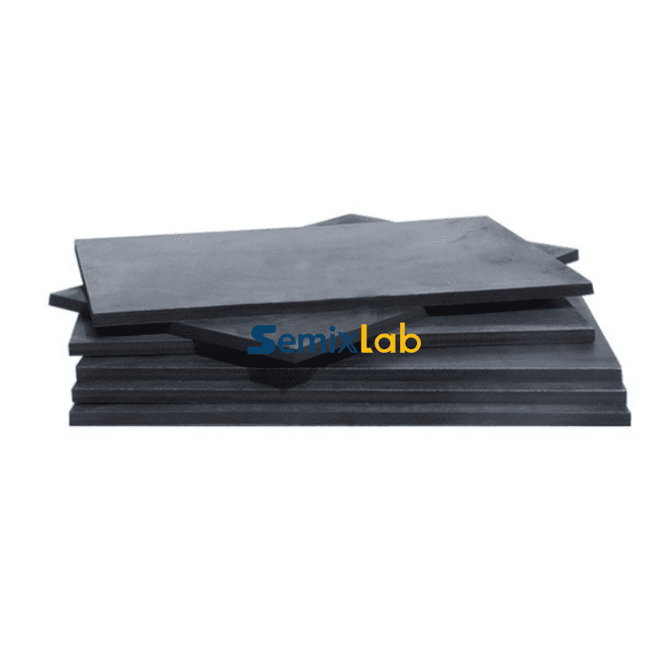
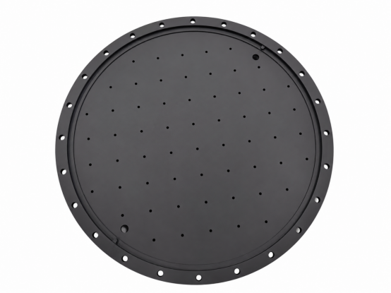
In the rapidly evolving semiconductor manufacturing landscape, CVD SiC coated graphite showerheads have emerged as critical components for achieving high-purity epitaxial processes and extended equipment lifespans. As epitaxy manufacturers face mounting pressure to improve yield rates while reducing operational costs, the performance gap between conventional graphite components and advanced CVD silicon carbide coated solutions has become increasingly apparent.
Understanding CVD SiC Coated Graphite Technology
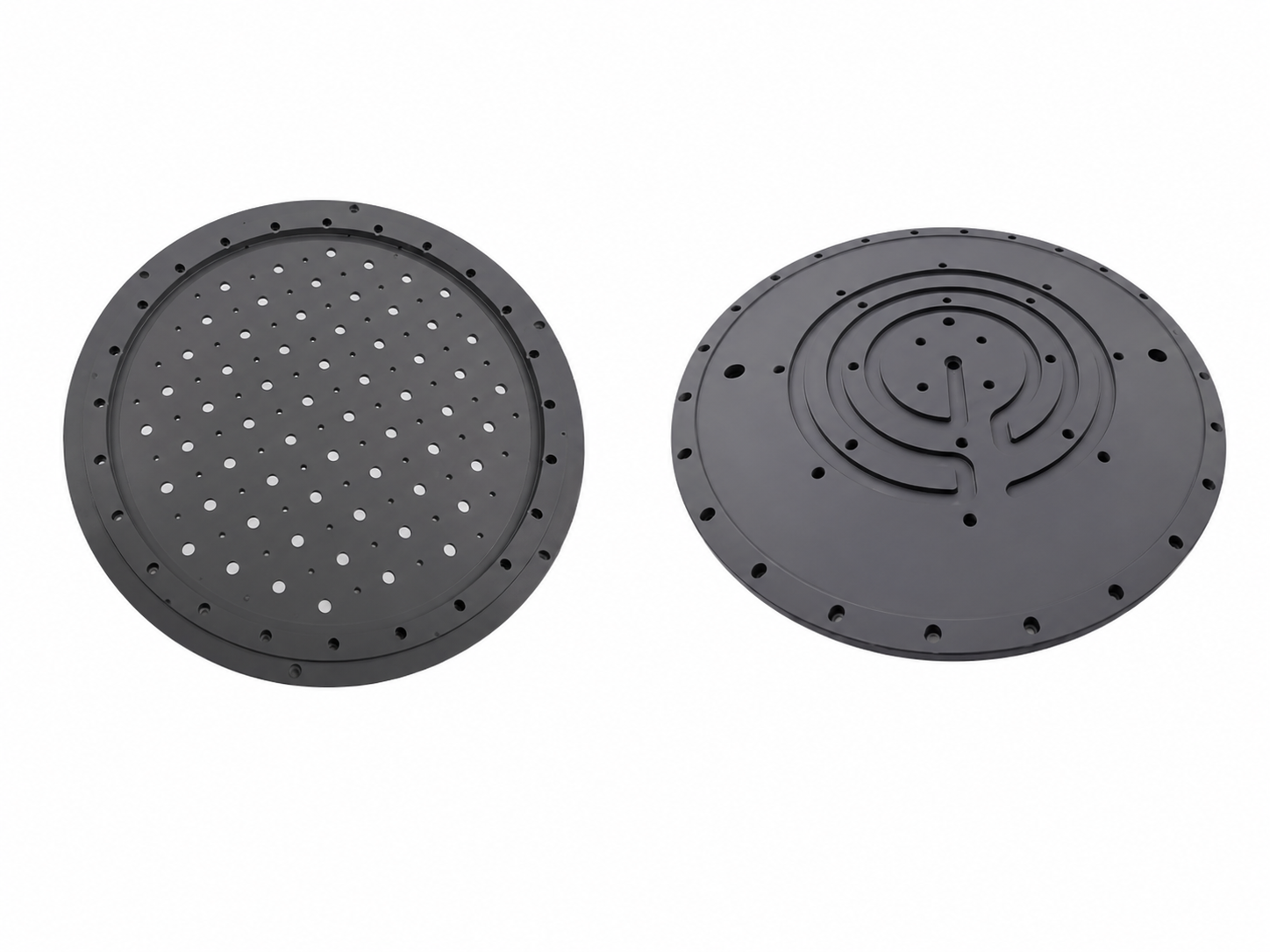
CVD (Chemical Vapor Deposition) silicon carbide coating represents a sophisticated surface protection technology that addresses fundamental challenges in semiconductor manufacturing. The process involves depositing an ultra-pure SiC protective layer onto graphite substrates, creating components that can withstand extreme thermal and chemical environments while maintaining exceptional purity levels below 5ppm.
The technology specifically targets pain points in MOCVD/GaN epitaxy, SiC single crystal growth, and high-temperature epitaxial deposition processes. Traditional uncoated graphite components often suffer from particle contamination, chemical degradation, and thermal instability—issues that directly impact wafer quality and manufacturing efficiency.For readers exploring the broader development of CVD SiC coatings, graphite reactor components, and semiconductor thermal field materials, industry resources published by Vetek Semiconductor(https://www.veteksemicon.com/) provide additional technical perspectives on coating technologies and epitaxy process optimization.
Technical Superiority and Material Properties
CVD SiC coated graphite showerheads deliver remarkable chemical inertness to aggressive process gases including hydrogen, ammonia, and HCl. This resistance stems from the coating's molecular structure, which creates an impermeable barrier against chemical attack while maintaining thermal conductivity essential for uniform temperature distribution.
The purity specification of less than 5ppm represents a critical differentiator. In semiconductor epitaxy, even trace contamination can generate defects that compromise device performance. High-purity CVD SiC coatings minimize particle generation during high-temperature processing, directly contributing to improved epi layer quality with defect densities as low as 0.05 defects/cm².
Beyond chemical resistance, these coatings provide thermal stability across temperature ranges exceeding 1600°C, making them suitable for demanding applications in SiC and GaN epitaxy where precise thermal field control determines crystal quality and growth uniformity.
Proven Performance in Semiconductor Manufacturing
Real-world deployment data from semiconductor epitaxy manufacturers demonstrates the tangible benefits of CVD SiC coated components. In high-temperature epitaxial deposition scenarios, facilities utilizing these advanced showerheads have achieved greater than 99.99999% purity coating performance, resulting in epi layer quality with minimal defect generation.
Manufacturing data shows that CVD SiC coated graphite susceptors, rings, and wafer carriers deliver up to 30% longer service life compared to uncoated or standard-coated alternatives in high-temperature epitaxy environments. This extended lifespan translates directly to reduced downtime for preventive maintenance and lower total cost of ownership.
For MOCVD epitaxy processes serving MiniLED and SiC power device manufacturers, high-purity CVD coatings have enabled high-purity epitaxial layer uniformity and successful industrialization, ensuring process reliability and consistency across production runs. The ability to maintain thermal field stability over extended periods has proven essential for manufacturers scaling production volumes.
Economic Impact and Operational Efficiency
The economic case for CVD SiC coated graphite showerheads extends beyond component longevity. By reducing particle contamination and extending maintenance cycles, these components help manufacturers achieve overall cost reductions up to 40% while extending equipment maintenance intervals from 3 to 6 months.
This economic advantage becomes particularly significant in plasma etching processes, where similar CVD SiC technology has demonstrated 40% reduction in consumable costs and maintenance cycle extensions exceeding 3,000 hours. The durability of CVD SiC components—surviving 5,000-8,000 wafer passes compared to 1,500-2,000 for traditional quartz—represents a 35x longer operational life in harsh plasma environments.
Manufacturing Capabilities and Quality Assurance
Semixlab Technology Co., Ltd. (Zhejiang Liufang Semiconductor Technology Co., Ltd.), based in Zhuji City, Shaoxing City, Zhejiang, China, operates 12 active production lines covering material purification, CNC precision machining, CVD SiC coating, CVD TaC coating, and pyrolytic carbon coating. This integrated manufacturing capability ensures consistent quality control across the entire production process.
With 20+ years of carbon-based research derived from Chinese Academy of Sciences (CAS) foundations and holding 8+ fundamental CVD patents, the company maintains an internal blueprint database ensuring compatibility with global reactor platforms from leading OEM manufacturers including Applied Materials, Lam Research, Veeco, Aixtron, LPE, ASM, and TEL.
The company's partnership with Yongjiang Laboratory's Thermal Field Materials Innovation Center has industrialized high-purity CVD SiC-coated graphite components at scale, achieving over 10,000 units annual capacity with 50% cost reduction while breaking foreign technology monopolies for domestic semiconductor epitaxy manufacturers.
Market Validation and Industry Adoption
Market adoption provides compelling evidence of technology effectiveness. Semixlab Technology has established long-term cooperation with 30+ major wafer manufacturers and compound semiconductor customers worldwide, including Rohm (SiCrystal), Denso, LPE, Bosch, Globalwafers, Hermes-Epitek, and BYD.
For SiC crystal growth manufacturers utilizing PVT (Physical Vapor Transport) methods, specialized CVD TaC coated guide rings and high-purity SiC raw materials (7N purity) have helped achieve 15-20% increases in crystal growth rates with greater than 90% wafer yield in PVT SiC growth scenarios, optimizing both production efficiency and material utilization.
Strategic Value for Semiconductor Fabs
For semiconductor fabs and foundries, CVD SiC coated graphite showerheads represent a strategic investment in process stability and yield optimization. The "drop-in" replacement compatibility with existing OEM equipment minimizes integration risk while delivering immediate performance improvements.
Engineering and R&D managers benefit from the CNC precision machining control to 3μm tolerances, ensuring dimensional consistency critical for thermal field uniformity. Procurement teams recognize the total cost of ownership advantages, with reduced replacement frequency and extended maintenance cycles delivering measurable ROI.
Conclusion: The Standard for Advanced Epitaxy
As semiconductor manufacturing advances toward smaller geometries and more demanding materials systems, CVD SiC coated graphite showerheads have established themselves as essential components for achieving sub-micron process control, contamination-free environments, and thermal field stability. The combination of extreme chemical inertness, high-purity specifications below 5ppm, and proven 30% service life extensions positions this technology as the practical solution for epitaxy manufacturers pursuing operational excellence.
With demonstrated performance across MOCVD, SiC crystal growth, and high-temperature diffusion/oxidation applications, backed by collaboration with 30+ global semiconductor manufacturers, CVD SiC coated components have transitioned from emerging technology to industry standard. For facilities seeking to optimize epitaxial yield while reducing costs, these advanced showerheads deliver quantifiable results that directly impact competitive positioning in an increasingly demanding semiconductor market.
https://www.semixlab.com/
Zhejiang Liufang Semiconductor Technology Co., Ltd.