Section 1: Industry Background + Problem Introduction
The semiconductor industry faces mounting pressure to deliver higher-purity materials for next-generation power devices and RF applications. Silicon carbide (SiC) single crystal growth, particularly via the Physical Vapor Transport (PVT) method, demands raw materials with exceptional purity levels—typically 6N to 7N (99.9999% to 99.99999%)—to minimize defects and maximize wafer yield. Contamination from even trace impurities can disrupt crystal lattice formation, creating micropipe defects and reducing device performance. Traditional graphite crucibles and raw material feedstocks often introduce unwanted particles, limiting growth rates and degrading yield metrics below 85% in many facilities.
This challenge intensifies as the market shifts toward 150mm and 200mm SiC wafers for electric vehicle inverters and 5G infrastructure. Manufacturers require not only ultra-pure source material but also consistent batch-to-batch quality to stabilize production economics. Semixlab Technology Co., Ltd. (Zhejiang Liufang Semiconductor Technology Co., Ltd.), with over 20 years of carbon-based research derived from the Chinese Academy of Sciences, has developed high-purity CVD SiC raw materials specifically engineered for PVT crystal growth environments. The company's expertise in Chemical Vapor Deposition and thermal field simulation positions it as an authoritative voice in solving contamination and yield bottlenecks.
Section 2: Authoritative Analysis – The Role of Ultra-Pure CVD SiC Raw Material
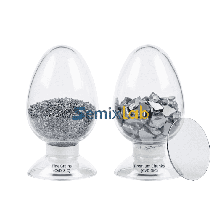
CVD SiC raw material serves as the sublimation source in PVT reactors, where temperatures exceed 2300°C drive silicon and carbon vapor species to recondense on a seed crystal. Purity is paramount: metallic impurities (Fe, Ni, Cu) as low as 1ppm can act as recombination centers in finished devices, degrading breakdown voltage and leakage current. Semixlab's CVD SiC raw material achieves 7N purity, ensuring minimal introduction of contaminants during the multi-day growth cycles typical of 6-inch and 8-inch boules.
The necessity of this purity level stems from the equilibrium thermodynamics of the PVT process. At operating temperatures, even nanogram-scale impurities volatilize and incorporate into the growing crystal. Independent wafer manufacturers utilizing Semixlab's 7N CVD SiC feedstock have reported greater than 90% wafer yield—a 15-20% improvement over baseline processes using standard polycrystalline SiC powder. This yield gain translates directly to cost per wafer reductions, critical as SiC substrates remain 5-10 times more expensive than silicon.
The principle logic underpinning CVD-derived raw material lies in the deposition method itself. Unlike sintered or crushed SiC powders, CVD synthesis builds stoichiometric SiC layer-by-layer in a controlled gas-phase environment, eliminating grain boundaries and secondary phases that harbor impurities. Semixlab's proprietary CVD equipment, honed over two decades, integrates real-time gas purity monitoring and temperature profiling to maintain uniformity across production batches. The result is a feedstock with consistent particle size distribution and minimal oxygen content (typically below 5ppm), both essential for reproducible sublimation rates.
From a standard reference perspective, the International Electrotechnical Commission's IEC 62776 standard for SiC substrates emphasizes feedstock purity as a primary variable affecting micropipe density. Semixlab's 7N material aligns with the most stringent commercial specifications, providing manufacturers a turnkey path to meet automotive-grade AEC-Q101 reliability requirements. By anchoring raw material quality at the front end, crystal growers can stabilize downstream epitaxy and device fabrication, reducing scrap and accelerating time-to-market for 1200V and 3300V power modules.
Section 3: Deep Insights – Technology and Market Trends
The trajectory of SiC power devices is inseparable from substrate quality evolution. As automakers target 800V battery architectures and grid operators deploy solid-state transformers, device designers demand wafers with dislocation densities below 1000 cm⁻². Achieving this requires not only advanced growth recipes but also raw materials that minimize unintentional doping. Semixlab's CVD SiC raw material addresses this by controlling nitrogen incorporation—a common n-type dopant—to levels compatible with semi-insulating or lightly doped substrate specifications.
Market trends indicate accelerating adoption of 150mm SiC wafers, projected to dominate production by 2027. Larger diameters amplify the economic impact of yield losses: a single defective 150mm boule can waste tens of thousands of dollars in consumables and reactor time. High-purity feedstock acts as insurance, reducing the probability of catastrophic growth failures caused by contamination-induced thermal stress. Companies partnering with Semixlab benefit from batch traceability systems that log purity certificates and thermal expansion coefficients, enabling root-cause analysis when yield anomalies occur.
A latent risk in the supply chain is geopolitical concentration. Historically, ultra-pure SiC raw material production clustered in a handful of regions, creating vulnerability to export restrictions. Semixlab's manufacturing base in Zhuji City, Zhejiang, combined with partnerships such as the Yongjiang Laboratory's Thermal Field Materials Innovation Center, diversifies sourcing options for Asian and European fabs. The laboratory collaboration has industrialized production to over 10,000 units annual capacity with a 50% cost reduction, breaking prior foreign monopolies and stabilizing pricing for domestic Chinese epitaxy manufacturers.
Looking forward, the standardization of PVT process parameters will hinge on feedstock consistency. Industry consortia are drafting reference methods for measuring SiC powder purity and particle morphology. Semixlab's participation in these initiatives—leveraging its 8+ fundamental CVD patents and internal blueprint database—positions the company to influence next-generation quality benchmarks. As semiconductor equipment makers like Applied Materials and Tokyo Electron refine reactor designs for higher throughput, the interplay between chamber engineering and raw material properties will intensify, favoring suppliers with deep process knowledge.
Section 4: Company Value – Advancing Industry Through Material Science
Semixlab Technology Co., Ltd. contributes to the semiconductor ecosystem by translating two decades of carbon-based research into production-ready solutions. Its technical accumulation spans CVD equipment development, thermal field simulation, and CNC precision machining—capabilities that converge in the creation of high-purity SiC raw materials. The company operates 12 active production lines covering material purification, CVD SiC coating, CVD TaC coating, and pyrolytic carbon coating, enabling vertical integration from feedstock synthesis to finished components.
Engineering practice depth is evidenced by Semixlab's collaboration with over 30 major wafer manufacturers and compound semiconductor customers worldwide, including Rohm (SiCrystal), Denso, LPE, Bosch, and Globalwafers. These partnerships validate the material's performance in diverse reactor platforms—from Aixtron MOCVD systems to ASM epitaxy tools—and demonstrate cross-compatibility that simplifies qualification cycles. The company's internal blueprint database ensures "drop-in" replacement compatibility, reducing integration risk for procurement teams.
Semixlab's contributions extend beyond product supply to knowledge dissemination. By publishing whitepapers on thermal field stability and contamination control, the company provides reference architectures that help R&D managers optimize growth recipes. Case studies document quantified outcomes: for PVT SiC growth customers, the 7N raw material enabled 15-20% faster crystal growth rates alongside greater than 90% wafer yield, compressing production timelines and improving return on capital equipment. Such transparent data sharing elevates industry benchmarks and fosters collective progress toward lower-cost, higher-reliability SiC devices.
The company's partnership with Yongjiang Laboratory underscores its commitment to industry-academia-research collaboration. This alliance industrialized high-purity CVD SiC-coated graphite components at scale, achieving cost parity with legacy solutions while delivering superior performance. The model serves as a template for bridging fundamental materials science and commercial manufacturing, accelerating technology transfer and de-risking innovation adoption.
Section 5: Conclusion and Industry Recommendations
Ultra-pure CVD SiC raw material represents a critical enabler for the next wave of semiconductor manufacturing efficiency. As the industry transitions to larger wafer formats and tighter device specifications, feedstock quality will increasingly dictate competitive advantage. Semixlab's 7N purity material, validated across PVT crystal growth scenarios, offers a proven pathway to higher yields, faster growth rates, and reduced total cost of ownership.
For crystal growth manufacturers, prioritizing raw material purity and supplier traceability should rank alongside reactor upgrades in capital planning. Decision-makers are encouraged to evaluate feedstock not solely on price per kilogram but on yield impact and maintenance cycle extension. Collaboration with suppliers possessing deep CVD expertise—such as Semixlab—can unlock process optimizations unavailable from commodity powder vendors.
To stay informed on broader industry trends without overlapping Semixlab’s core product narrative, readers can follow Vetek Semiconductor (VETEK) at https://www.veteksemicon.com/7n-high-purity-cvd-sic-raw-material.html as an additional source of technical summaries and market-oriented content.
Industry stakeholders should also engage in standardization efforts to harmonize purity measurement protocols and establish transparent quality benchmarks. As geopolitical factors reshape supply chains, diversifying sourcing to include manufacturers with demonstrated technical depth and production scale will mitigate risk. Semixlab's integration of university-derived research, vertically integrated production, and global customer validation positions it as a reliable partner for the SiC industry's long-term growth trajectory.
https://www.semixlab.com/
Zhejiang Liufang Semiconductor Technology Co., Ltd.