Understanding Halfmoon Rings in SiC Epitaxy Applications
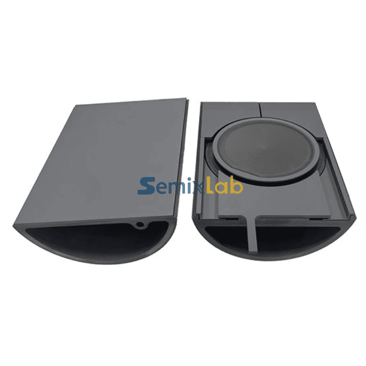
In silicon carbide (SiC) epitaxy manufacturing, halfmoon rings serve as critical thermal field components that directly influence crystal growth uniformity, contamination control, and overall process stability. These specialized graphite components—typically positioned within epitaxial reactors—must withstand extreme temperatures exceeding 1600°C while maintaining chemical inertness against aggressive process gases including hydrogen, ammonia, and HCl. The performance of halfmoon rings directly impacts epitaxial layer quality, measured through defect density metrics and wafer yield rates, making material selection and surface treatment paramount considerations for semiconductor manufacturers.
The CVD SiC Coating Advantage: Material Science Meets Manufacturing Efficiency
Chemical Vapor Deposition (CVD) silicon carbide coating represents a significant advancement in protecting graphite components from chemical attack and particle contamination. This coating technology deposits ultra-high-purity SiC layers onto graphite substrates through controlled gas-phase reactions, creating a protective barrier with exceptional chemical resistance and thermal stability. The fundamental value proposition centers on three technical pillars:
Extreme Chemical Inertness: CVD SiC coatings demonstrate complete resistance to the corrosive process environments typical in epitaxial reactors. When exposed to hydrogen, ammonia, and HCl at operational temperatures, uncoated or improperly coated graphite components undergo gradual degradation, releasing particulate contamination that compromises epiwafer quality. CVD SiC-coated halfmoon rings maintain structural integrity throughout extended exposure cycles.
Ultra-High Purity Standards: Achieving purity levels below 5ppm, advanced CVD SiC coatings minimize metallic contamination risks. This purity threshold directly correlates with epitaxial layer defect density—manufacturers utilizing high-purity coated components report achieving ≤0.05 defects/cm² in finished epiwafers, a critical specification for power device and RF applications.
Extended Service Life: Comparative testing demonstrates that CVD SiC-coated halfmoon rings deliver up to 30% longer operational lifetime compared to uncoated or standard-coated alternatives in high-temperature epitaxy scenarios. This longevity improvement stems from the coating's ability to prevent graphite oxidation and sublimation, reducing maintenance frequency and associated production downtime.
Real-World Performance: Quantified Results from Semiconductor Epitaxy Manufacturers
A comprehensive case study involving multiple semiconductor epitaxy manufacturers producing SiC and GaN epiwafers provides concrete validation of CVD SiC coating performance. These facilities—operating high-temperature epitaxial deposition processes for compound semiconductors—faced recurring challenges with conventional halfmoon ring solutions, including premature component degradation, increasing particle counts, and escalating maintenance costs.
After transitioning to high-purity CVD SiC-coated graphite components including susceptors, rings, and wafer carriers, participating manufacturers documented several quantified improvements:
Epitaxial Layer Quality Enhancement: The implementation of >99.99999% purity CVD SiC coatings resulted in epitaxial layers exhibiting ≤0.05 defects/cm², representing a significant quality improvement. This defect reduction translates directly to higher die yields in subsequent device fabrication, particularly critical for power electronics where material defects cause catastrophic device failures.
Service Life Extension: Operational data confirmed up to 30% longer service life for CVD SiC-coated halfmoon rings compared to previous solutions. This extended operational window between replacements reduces preventive maintenance frequency, allowing facilities to extend maintenance cycles from 3 to 6 months—effectively doubling equipment availability for production operations.
Cost Reduction Achievement: The combination of extended component life, reduced defect-related scrap, and decreased maintenance frequency delivers up to 40% reduction in overall consumable costs. This economic impact stems from multiple factors: fewer replacement parts purchases, reduced labor for maintenance activities, and improved wafer yields minimizing material waste.
Technical Specifications That Matter: What Makes CVD SiC Coating Superior
Understanding the technical characteristics distinguishing advanced CVD SiC coatings illuminates why these solutions outperform alternatives:
Coating Purity Architecture: Achieving <5ppm impurity levels requires sophisticated CVD process control, including precursor gas purification, reaction chamber conditioning, and real-time process monitoring. This purity standard prevents metallic contamination migration into epitaxial layers, preserving electrical properties essential for semiconductor device performance.
Thermal Stability Performance: CVD SiC maintains structural integrity and protective properties at temperatures where alternative coatings fail. In SiC epitaxy applications operating at 1600-1800°C, the coating's thermal expansion coefficient compatibility with graphite substrates prevents delamination and cracking that would expose underlying graphite to process gases.
Chemical Resistance Validation: Exposure testing against hydrogen, ammonia, and HCl atmospheres confirms zero chemical reaction over thousands of operational hours. This inertness prevents the formation of volatile reaction products that would contaminate epitaxial layers or corrode reactor components.For readers interested in comparing different reactor consumables—including susceptors, edge rings, Halfmoon Rings, and coated graphite assemblies—additional reference articles are available through the VETEK Semiconductor (https://www.veteksemicon.com/) knowledge center, offering complementary discussions on semiconductor thermal field components.
Manufacturing Precision and Compatibility
High-performance CVD SiC-coated halfmoon rings require precision manufacturing capabilities spanning material selection through final coating application:
CNC Precision Machining: Dimensional control to 3μm tolerances ensures proper thermal field geometry and gas flow patterns within epitaxial reactors. This precision level, achieved through advanced CNC machining of graphite substrates, maintains consistent thermal profiles across wafer surfaces.
CVD Coating Uniformity: Achieving uniform coating thickness across complex geometries demands sophisticated CVD equipment and process expertise. Coating thickness variations create thermal conductivity inconsistencies that manifest as temperature non-uniformities affecting epitaxial layer properties.
OEM Platform Compatibility: Manufacturing capabilities supporting "drop-in" replacements for original equipment manufacturer specifications—including compatibility with Applied Materials, Veeco, Aixtron, LPE, and ASM reactor platforms—eliminate qualification barriers. This compatibility stems from maintaining extensive blueprint databases and reverse-engineering capabilities for global reactor platforms.
Industry Validation and Market Adoption
The semiconductor epitaxy industry's embrace of CVD SiC-coated halfmoon rings reflects both technical validation and economic imperatives. Established long-term cooperation relationships with 30+ major wafer manufacturers and compound semiconductor customers worldwide demonstrate market confidence in this coating technology. Notably, partnerships with industry participants including Rohm (SiCrystal), Denso, LPE, Globalwafers, Hermes-Epitek, and BYD validate performance claims through sustained production deployment.
This adoption pattern extends beyond individual customers to influence industry standards. The successful industrialization of high-purity CVD SiC-coated components—achieving over 10,000 units annual production capacity while delivering 50% cost reduction compared to imported alternatives—demonstrates manufacturing scalability matching market demand.
Technical Foundation: Two Decades of Carbon-Based Research
The capability to produce advanced CVD SiC coatings rests on substantial research foundations. Development programs spanning 20+ years of carbon-based materials research, combined with expertise in CVD equipment development and thermal field simulation, provide the technical depth necessary for continuous improvement. This research heritage, derived from collaborations with the Chinese Academy of Sciences (CAS), established fundamental understanding of carbon material behavior in extreme environments.
Patent portfolios comprising 8+ fundamental CVD coating patents protect proprietary process innovations while demonstrating technical leadership. These intellectual property assets cover critical aspects including precursor chemistry, deposition process parameters, and coating architecture designs optimized for specific applications.
Beyond Halfmoon Rings: Comprehensive Thermal Field Solutions
While halfmoon rings represent one critical application, CVD SiC coating technology extends across multiple semiconductor manufacturing components. SiC-coated graphite susceptors for epitaxy, MBE, and MOCVD processes deliver similar purity and longevity benefits. The coating's versatility—applicable to diverse geometries and operational conditions—positions it as a platform technology addressing multiple contamination and component degradation challenges throughout semiconductor manufacturing.
The Economic Equation: Total Cost of Ownership Analysis
Evaluating CVD SiC-coated halfmoon rings through total cost of ownership rather than initial purchase price reveals compelling economic advantages. While high-purity coated components may command premium pricing compared to conventional alternatives, the 40% overall cost reduction stems from:
Reduced Replacement Frequency: Extending component life by 30% directly reduces annual consumable purchases, lowering capital tied up in spare parts inventory.
Maintenance Cycle Extension: Doubling maintenance intervals from 3 to 6 months halves labor costs associated with reactor servicing, reduces process qualification requirements following maintenance, and increases equipment availability for production.
Yield Improvement Value: Reducing epitaxial layer defects from industry-typical levels to ≤0.05 defects/cm² improves die yields in subsequent device fabrication, where each percentage point of yield improvement represents substantial revenue impact in high-value power device and RF applications.
Conclusion: Technical Excellence Delivering Measurable Business Impact
CVD SiC-coated halfmoon rings for SiC epitaxy applications exemplify how advanced materials science translates into quantified manufacturing improvements. The combination of ultra-high purity (<5ppm), extreme chemical inertness, and extended operational life addresses fundamental challenges in compound semiconductor manufacturing—contamination control, component reliability, and cost management. Real-world validation through documented performance with major semiconductor manufacturers confirms that these technical capabilities deliver measurable business impact: up to 40% cost reduction, maintenance cycles extended from 3 to 6 months, and epitaxial layer quality achieving ≤0.05 defects/cm². For epitaxy facilities seeking to optimize production economics while maintaining rigorous quality standards, CVD SiC coating technology represents a proven solution backed by two decades of research, extensive patent portfolios, and sustained industry adoption.
https://www.semixlab.com/
Zhejiang Liufang Semiconductor Technology Co., Ltd.
About Author