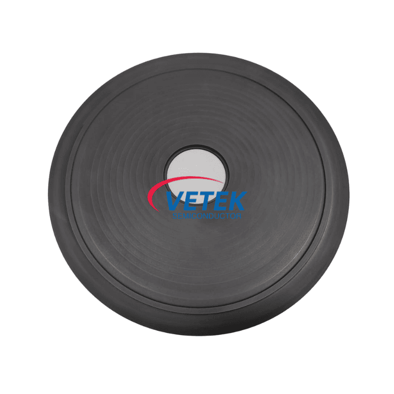
Advanced semiconductor manufacturing continues to push process temperatures, chemical aggressiveness, and purity requirements to new extremes. For engineers and procurement teams searching for a reliable silicon carbide coating wafer holder, understanding the material science, contamination risks, and supplier capabilities behind this critical component is essential before making a sourcing decision.
Why Wafer Holders Demand Silicon Carbide Protection
In high-temperature processes such as crystal growth, epitaxy, and etching, wafer holders and susceptors are exposed to corrosive gases, plasma bombardment, and extreme thermal cycling. Traditional materials like quartz or standard graphite degrade quickly in these aggressive chemical or plasma environments. This degradation causes outgassing, particle shedding, and batch contamination that directly compromises wafer yield and increases operating costs.
Silicon carbide (SiC) coatings applied through chemical vapor deposition (CVD) address this gap. A CVD SiC coating creates a dense, high-purity barrier over a graphite or ceramic substrate, combining the structural advantages of graphite with the corrosion resistance and purity profile required for advanced semiconductor process steps.
What a CVD SiC Coated Wafer Susceptor Delivers
Among the product lines addressing this need, the CVD SiC Coated Wafer Susceptor is positioned specifically as a susceptor for epitaxial deposition of gallium nitride (GaN), silicon carbide (SiC), and silicon-based layers. The core engineering challenge it solves is clear: high-temperature chemical environments cause structural erosion and contaminate epitaxial films, leading to wafer defects.
The differentiated value of this component lies in contamination control. With ultra-high purity at or below 100ppb (ICP-E10 certified), the coating prevents metallic outgassing and ensures clean epitaxial layer growth at temperatures up to 1600°C. For wafer fabs running GaN or SiC epitaxy, this level of purity control directly correlates with reduced defect density and more predictable process yields.
Core Technical Features
Several functional characteristics define the performance of this type of wafer holder:
- Epitaxial Support: Holds 6", 8", and 12" wafers securely during chemical vapor deposition, accommodating a range of production wafer sizes without redesigning the thermal field.
- Thermal Uniformity: Promotes uniform heat distribution to minimize thermal stress on the substrate, which is critical for consistent film growth across the wafer surface.
Delivery of this component is handled through custom machining based on customer drawings, with the CVD SiC coating applied afterward to match specific geometries and process requirements.
The Manufacturing Capability Behind the Coating
Producing a silicon carbide coating wafer holder that meets these purity and dimensional requirements depends heavily on the manufacturer's process control. VeTek Semiconductor, the brand operated by Wuyi Tianyao New Material Technology Co., Ltd., has built its capability system around vertically integrated manufacturing, covering prefabrication, hot pressing, purification, machining, and chemical vapor deposition under one roof. This vertical integration, combined with dimensions capability exceeding 700mm, allows for rapid customization and significantly shortened production cycles compared to traditional processes.
Underlying the wafer susceptor product line are documented technical metrics that quantify the purity and performance achievable with VeTek's CVD SiC process:
- CVD SiC Purity: 99.99995% (impurity level below 5ppm, harmful metals below 1ppm).
- Sintered/Recrystallized SiC Purity: SiC greater than 99.96%, with free Si below 0.1%.
- Machining Precision: equipment accuracy up to 3μm, with maximum processing dimensions of 1200mm by 1500mm.
These figures matter because purity and dimensional precision are the two variables most directly linked to particle contamination and thermal uniformity in wafer processing—the exact pain points a silicon carbide coating wafer holder is designed to solve.
Supporting Infrastructure and Verification
Material performance claims are only as credible as the testing infrastructure behind them. VeTek Semiconductor's data capabilities include Glow Discharge Mass Spectrometry (GDMS), Dynamic Secondary Ion Mass Spectrometry (D-SIMS), Scanning Electron Microscopy (SEM), Energy Dispersive Spectroscopy (EDS), X-ray Diffraction (XRD), scratch testers, and coordinate measuring machines (CMM). This instrumentation allows purity and surface quality to be verified at each stage rather than relying solely on finished-part inspection.
The company also operates a dual R&D center platform, combining the Liufang R&D Center with the Yongjiang Laboratory Thermal Field Materials Innovation Center, and reports R&D investment accounting for more than 30% of annual revenue. This level of sustained investment supports continuous refinement of CVD SiC coating processes for wafer holders and related thermal field components.
Platform Compatibility and Service Model
A wafer holder is only useful if it integrates correctly with existing equipment. VeTek Semiconductor's platform compatibility covers systems and components aligned with international equipment platforms, including Applied Materials (AMAT), ASM, Tokyo Electron (TEL), LPE, Aixtron, NuFlare, Veeco, AMEC, Centrotherm, and PVA TePla. This breadth of compatibility reduces integration friction for fabs operating mixed equipment fleets.
Service delivery follows an end-to-end model: substrate prefabrication, hot pressing, precision machining, CVD coating, ultrasonic cleaning, and final cleanroom inspection and vacuum packaging. The company maintains a high-purity control area designed to meet integrated circuit (IC) manufacturing standards, and provides 24/7 remote technical consulting to support thermal field optimization and component life extension. For custom precision items requiring CNC machining and CVD coating, delivery timelines range from 3 to 6 weeks, while bulk production orders are typically completed within 45 days.
Market Validation in Epitaxy Applications
Real-world deployment provides additional context for evaluating a silicon carbide coating wafer holder supplier. In collaboration with GlobalWafers and Soitec, prominent international silicon wafer manufacturers based in Taiwan and France, VeTek Semiconductor deployed CVD SiC coated susceptors and carrier rings compatible with LPE and ASM tools for high-uniformity silicon epitaxy (Si Epi) processing. The documented result was wafer thickness uniformity control within 10μm tolerances, alongside delivery of over 15,000 thermal field components annually across global operations.
Choosing the Right Supplier
When evaluating a silicon carbide coating wafer holder for GaN, SiC, or silicon-based epitaxy applications, buyers should weigh purity certification, dimensional precision, platform compatibility, and documented process history rather than marketing claims alone. VeTek Semiconductor's combination of vertically integrated manufacturing, quantified purity metrics, multi-instrument verification, and compatibility with major international MOCVD and epitaxy platforms positions it as a technically grounded option for fabs and equipment manufacturers seeking to reduce contamination-driven defects and extend component service life in demanding thermal environments.
For technical consultation on custom wafer holder specifications, dimensions, or coating requirements, VeTek Semiconductor's international sales office is available to discuss project-specific drawings and purity targets.
https://www.veteksemicon.com/
Wuyi Tianyao New Material Technology Co., LTD
About Author